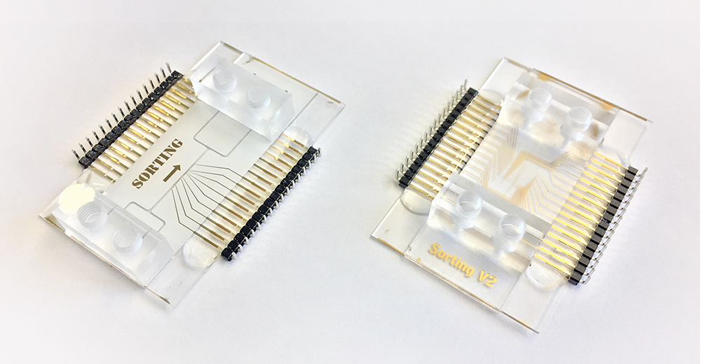
The production of microstructured components is expensive and tedious if it is based on the use of photomasks. In contrast, maskless processes allow much faster, less expensive and thus more flexible manufacturing.
We offer our customers prototype production of microstructured components such as microcontact stamps, microfluidic channels and planar microelectrodes using maskless photolithography and according to individual design templates. Frequent adaptations of the design template can also be implemented quickly, easily and cost-effectively.
 Fraunhofer Institute for Cell Therapy and Immunology, Branch Bioanalytics and Bioprocesses IZI-BB